Product Description
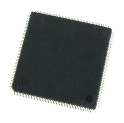
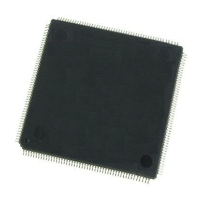
A3P250-PQG208I Programmable Logic ICs FPGA Field Programmable Gate Array A3P250-PQG208I LEAD FREE
Features and Benefits
High Capacity
• 15 K to 1 M System Gates
• Up to 144 Kbits of True Dual-Port SRAM
• Up to 300 User I/Os Reprogrammable Flash Technology
• 130-nm, 7-Layer Metal (6 Copper), Flash-Based CMOS Process
• Instant On Level 0 Support
• Single-Chip Solution
• Retains Programmed Design when Powered Off High Performance
• 350 MHz System Performance
• 3.3 V, 66 MHz 64-Bit PCI† In-System Programming (ISP) and Security
• ISP Using On-Chip 128-Bit Advanced Encryption Standard (AES) Decryption (except ARM®-enabled ProASIC®3 devices) via JTAG (IEEE 1532–compliant)† • FlashLock® to Secure FPGA Contents Low Power
• Core Voltage for Low Power
• Support for 1.5 V-Only Systems
• Low-Impedance Flash Switches High-Performance Routing Hierarchy
• Segmented, Hierarchical Routing and Clock Structure
Advanced I/O
• 700 Mbps DDR, LVDS-Capable I/Os (A3P250 and above)
• 1.5 V, 1.8 V, 2.5 V, and 3.3 V Mixed-Voltage Operation
• Wide Range Power Supply Voltage Support per JESD8-B, Allowing I/Os to Operate from 2.7 V to 3.6 V
• Bank-Selectable I/O Voltages—up to 4 Banks per Chip
• Single-Ended I/O Standards: LVTTL, LVCMOS 3.3 V / 2.5 V / 1.8 V / 1.5 V, 3.3 V PCI / 3.3 V PCI-X† and LVCMOS 2.5 V / 5.0 V Input
• Differential I/O Standards: LVPECL, LVDS, B-LVDS, and M-LVDS (A3P250 and above) • I/O Registers on Input, Output, and Enable Paths • Hot-Swappable and Cold Sparing I/Os‡
• Programmable Output Slew Rate† and Drive Strength
• Weak Pull-Up/-Down
• IEEE 1149.1 (JTAG) Boundary Scan Test
• Pin-Compatible Packages across the ProASIC3 Family Clock Conditioning Circuit (CCC) and PLL†
• Six CCC Blocks, One with an Integrated PLL
• Configurable Phase-Shift, Multiply/Divide, Delay Capabilities and External Feedback
• Wide Input Frequency Range (1.5 MHz to 350 MHz) Embedded Memory†
• 1 Kbit of FlashROM User Nonvolatile Memory
• SRAMs and FIFOs with Variable-Aspect-Ratio 4,608-Bit RAM Blocks (×1, ×2, ×4, ×9, and ×18 organizations)†
• True Dual-Port SRAM (except ×18) ARM Processor Support in ProASIC3 FPGAs
• M1 ProASIC3 Devices—ARM®Cortex®-M1 Soft Processor Available with or without Debug

 Your message must be between 20-3,000 characters!