Product Description
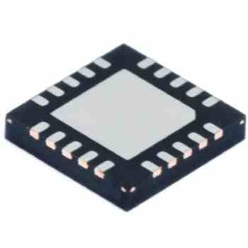
LTC6406IUDTRPBF High Speed Operational Amplifiers 800 MHz Low Noise Rail Input Differential Amplifier Driver
ELECTRICAL CHARACTERISTICS
Note 1: Stresses beyond those listed under Absolute Maximum Ratings may cause permanent damage to the device. Exposure to any Absolute Maximum Rating condition for extended periods may affect device reliability and lifetime.
Note 2: Input pins (+IN, –IN, VOCM, SHDN and VTIP) are protected by steering diodes to either supply. If the inputs should exceed either supply voltage, the input current should be limited to less than 10mA. In addition, the inputs +IN, –IN are protected by a pair of back-to-back diodes. If the differential input voltage exceeds 1.4V, the input current should be limited to less than 10mA.
Note 3: A heat sink may be required to keep the junction temperature below the Absolute Maximum Rating when the output is shorted indefi nitely. Long-term application of output currents in excess of the absolute maximum ratings may impair the life of the device.
Note 4: The LTC6406C/LTC6406I are guaranteed functional over the operating temperature range –40°C to 85°C.
Note 5: The LTC6406C is guaranteed to meet specifi ed performance from 0°C to 70°C. The LTC6406C is designed, characterized, and expected to meet specifi ed performance from –40°C to 85°C but is not tested or QA sampled at these temperatures. The LTC6406I is guaranteed to meet specifi ed performance from –40°C to 85°C.
Note 6: Input bias current is defi ned as the average of the input currents fl owing into the inputs (–IN, and +IN). Input offset current is defi ned as the difference between the input currents (IOS = IB + – IB –).
Note 7: Input common mode range is tested using the test circuit of Figure 1 by taking three measurements of differential gain with a ±1V DC differential output with VICM = 0V; VICM = 1.25V; VICM = 3V, verifying that the differential gain has not deviated from the VICM = 1.25V case by more than 0.5%, and that the common mode offset (VOSCM) has not deviated from the common mode offset at VICM = 1.25V by more than ±20mV. The voltage range for the output common mode range is tested using the test circuit of Figure 1 by applying a voltage on the VOCM pin and testing at both VOCM = 1.25V and at the Electrical Characteristics table limits to verify that the common mode offset (VOSCM) has not deviated by more than ±10mV from the VOCM = 1.25V case.
Note 8: Input CMRR is defi ned as the ratio of the change in the input common mode voltage at the pins +IN or –IN to the change in differential input referred voltage offset. Output CMRR is defi ned as the ratio of the change in the voltage at the VOCM pin to the change in differential input referred voltage offset. This specifi cation is strongly dependent on feedback ratio matching between the two outputs and their respective inputs, and it is diffi cult to measure actual amplifi er performance (see the Effects of Resistor Pair Mismatch in the Applications Information section of this data sheet). For a better indicator of actual amplifi er performance independent of feedback component matching, refer to the PSRR specifi cation.
Note 9: Differential power supply rejection (PSRR) is defi ned as the ratio of the change in supply voltage to the change in differential input referred voltage offset. Common mode power supply rejection (PSRRCM) is defi ned as the ratio of the change in supply voltage to the change in the common mode offset, VOUTCM – VOCM.
Note 10: Extended operation with the output shorted may cause the junction temperature to exceed the 150°C limit.
Note 11: Because the LTC6406 is a feedback amplifi er with low output impedance, a resistive load is not required when driving an ADC. Therefore, typical output power can be very small in many applications. In order to compare the LTC6406 with RF style amplifi ers that require 50Ω load, the output voltage swing is converted to dBm as if the outputs were driving a 50Ω load. For example, 2VP-P output swing is equal to 10dBm using this convention.
Note 12: Includes offset/drift induced by feedback resistors mismatch. See the Applications Information section for more details. Note 13: QFN package only. Refer to data sheet curves for MSOP package numbers

 Your message must be between 20-3,000 characters!