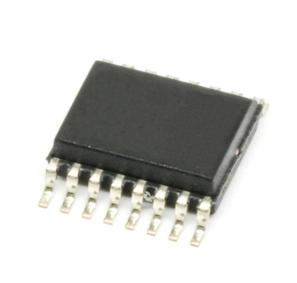
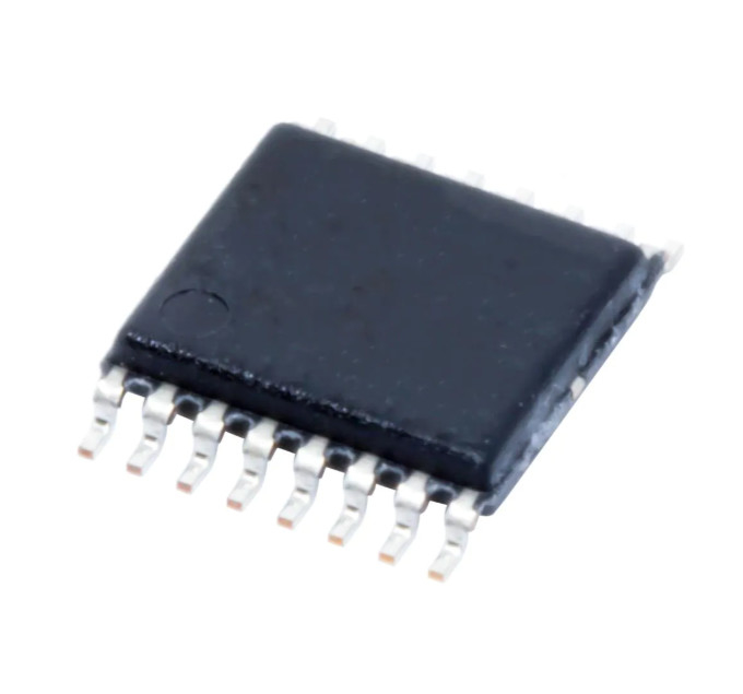
Product Description
AM26C32 Quadruple Differential Line Receiver
1 Features
• Meets or Exceeds the Requirements of ANSI TIA/EIA-422-B, TIA/EIA-423-B, and ITU Recommendation V.10 and V.11
• Low Power, ICC = 10 mA Typical
• ±7-V Common-Mode Range With ±200-mV Sensitivity
• Input Hysteresis: 60 mV Typical
• tpd = 17 ns Typical
• Operates From a Single 5-V Supply
• 3-State Outputs
• Input Fail-Safe Circuitry
• Improved Replacements for AM26LS32 Device
• Available in Q-Temp Automotive
2 Applications
• High-Reliability Automotive Applications
• Factory Automation
• ATM and Cash Counters
• Smart Grid
• AC and Servo Motor Drives
3 Description
The AM26C32 device is a quadruple differential line receiver for balanced or unbalanced digital data transmission. The enable function is common to all four receivers and offers a choice of active-high or active-low input.
The 3-state outputs permit connection directly to a busorganized system. Fail-safe design specifies that if the inputs are open, the outputs always are high.
The AM26C32 devices are manufactured using a BiCMOS process, which is a combination of bipolar and CMOS transistors. This process provides the high voltage and current of bipolar with the low power of CMOS to reduce the power consumption to about one-fifth that of the standard AM26LS32, while maintaining AC and DC performance.
Device Information(1)
Pin Functions
|
PIN
|
I/O
|
DESCRIPTION
|
|
NAME
|
LCCC
|
SOIC, PDIP, SO, TSSOP, CFP, or CDIP
|
|
1A
|
3
|
2
|
I
|
RS422/RS485 differential input (noninverting)
|
|
1B
|
2
|
1
|
I
|
RS422/RS485 differential input (inverting)
|
|
1Y
|
4
|
3
|
O
|
Logic level output
|
|
2A
|
8
|
6
|
I
|
RS422/RS485 differential input (noninverting)
|
|
2B
|
9
|
7
|
I
|
RS422/RS485 differential input (inverting)
|
|
2Y
|
7
|
5
|
O
|
Logic level output
|
|
3A
|
13
|
10
|
I
|
RS422/RS485 differential input (noninverting)
|
|
3B
|
12
|
9
|
I
|
RS422/RS485 differential input (inverting)
|
|
3Y
|
14
|
11
|
O
|
Logic level output
|
|
4A
|
18
|
14
|
I
|
RS422/RS485 differential input (noninverting)
|
|
4B
|
19
|
15
|
I
|
RS422/RS485 differential input (inverting)
|
|
4Y
|
17
|
13
|
O
|
Logic level output
|
|
G
|
5
|
4
|
I
|
Active-high select
|
|
G
|
15
|
12
|
I
|
Active-low select
|
|
GND
|
10
|
8
|
—
|
Ground
|
|
NC(1)
|
1
|
—
|
—
|
Do not connect
|
|
6
|
|
11
|
|
16
|
|
VCC
|
20
|
16
|
—
|
Power Supply
|
(1) NC – no internal connection.
Specifications
4.1 Absolute Maximum Ratings
over operating free-air temperature range (unless otherwise noted) (1)
| |
MIN MAX |
UNIT |
| VCC Supply voltage(2) |
7 |
V |
| VI Input voltage |
A or B inputs |
–11 14 |
V
|
| G or G inputs |
–0.5 VCC + 0.5 |
| VID Differential input voltage |
–14 14 |
V |
| VO Output voltage |
–0.5 VCC + 0.5 |
V |
| IO Output current |
±25 |
mA |
| Tstg Storage temperature |
-65 150 |
°C |
(1) Stresses beyond those listed under Absolute Maximum Ratings may cause permanent damage to the device. These are stress ratings only, which do not imply functional operation of the device at these or any other conditions beyond those indicated under Recommended Operating Conditions. Exposure to absolute-maximum-rated conditions for extended periods may affect device reliability.
(2) All voltage values, except differential voltages, are with respect to the network ground terminal.
4.1 ESD Ratings
| |
VALUE |
UNIT |
|
V(ESD) Electrostatic discharge
|
Human body model (HBM), per ANSI/ESDA/JEDEC JS-001(1) |
±3000 |
V
|
| Charged-device model (CDM), per JEDEC specification JESD22- C101(2) |
±2000 |
(1) JEDEC document JEP155 states that 500-V HBM allows safe manufacturing with a standard ESD control process.
(2) JEDEC document JEP157 states that 250-V CDM allows safe manufacturing with a standard ESD control process.
4.2 Recommended Operating Conditions
over operating free-air temperature range (unless otherwise noted)
| |
MIN |
NOM |
MAX |
UNIT |
| VCC |
Supply voltage |
|
4.5 |
5 |
5.5 |
V |
| VIH |
High-level input voltage |
|
2 |
|
Vcc |
V |
| VIL |
Low-level input voltage |
|
0 |
|
0.8 |
V |
| VIC |
Common-mode input voltage |
|
-7 |
|
+7 |
V |
| IOH |
High-level output current |
|
–6 |
mA |
| IOL |
Low-level output current |
|
6 |
mA |
|
TA
|
Operating free-air temperature
|
AM26C32C |
0 |
|
70 |
°C
|
| AM26C32I |
–40 |
|
85 |
| AM26C32Q |
–40 |
|
125 |
| AM26C32M |
–55 |
|
125 |
4.3 Thermal Information
|
THERMAL METRIC(1)
|
AM26C32 |
UNIT
|
| D (SOIC) |
N (PDIP) |
NS (SO) |
PW (TSSOP) |
| 16 PINS |
16 PINS |
16 PINS |
16 PINS |
| RθJA Junction-to-ambient thermal resistance |
73 |
67 |
64 |
108 |
°C/W |
(1) For more information about traditional and new thermal metrics, see the Semiconductor and IC Package Thermal Metrics application report, SPRA953.
4.1 Electrical Characteristics
over operating free-air temperature range (unless otherwise noted)
| PARAMETER |
TEST CONDITIONS |
MIN |
TYP(1) |
MAX |
UNIT |
| VIT+ |
Differential input high-threshold voltage |
VO = VOH(min), IOH = –440
µA
|
VIC = –7 V to 7 V |
0.2 |
V
|
| VIC = 0 V to 5.5 V |
0.1 |
| VIT– |
Differential input low-threshold voltage |
VO = 0.45 V, IOL = 8 mA |
VIC = –7 V to 7 V |
–0.2(2) |
V
|
| VIC = 0 V to 5.5 V |
–0.1(2) |
| Vhys |
Hysteresis voltage (VIT+ – VIT−) |
|
60 |
mV |
| VIK |
Enable input clamp voltage |
VCC = 4.5 V, II = –18 mA |
–1.5 |
V |
| VOH |
High-level output voltage |
VID = 200 mV, IOH = –6 mA |
3.8 |
V |
| VOL |
Low-level output voltage |
VID = –200 mV, IOL = 6 mA |
|
0.2 |
0.3 |
V |
| IOZ |
OFF-state (high-impedance state) output current |
VO = VCC or GND |
|
±0.5 |
±5 |
µA |
| II |
Line input current
|
VI = 10 V, Other input at 0 V |
1.5 |
mA |
| VI = –10 V, Other input at 0 V |
–2.5 |
mA |
| IIH |
High-level enable current |
VI = 2.7 V |
20 |
μA |
| IIL |
Low-level enable current |
VI = 0.4 V |
–100 |
μA |
| ri |
Input resistance |
One input to ground |
12 |
17 |
|
kΩ |
| ICC |
Quiescent supply current |
VCC = 5.5 V |
|
10 |
15 |
mA |
(1) All typical values are at VCC = 5 V, VIC = 0, and TA = 25°C.
(2) The algebraic convention, in which the less positive (more negative) limit is designated minimum, is used in this data sheet for common- mode input voltage.
4.1 Switching Characteristics
over operating free-air temperature range, CL = 50 pF (unless otherwise noted)
|
PARAMETER
|
TEST CONDITIONS
|
AM26C32C AM26C32I |
AM26C32Q AM26C32M |
UNIT
|
| MIN |
TYP(1) |
MAX |
MIN |
TYP(1) |
MAX |
| tPLH |
Propagation delay time, low- to high-level output |
See Figure 2
|
9 |
17 |
27 |
9 |
17 |
27 |
ns |
| tPHL |
Propagation delay time, high- to low-level output |
9 |
17 |
27 |
9 |
17 |
27 |
ns |
| tTLH |
Output transition time, low- to high-level output |
See Figure 2
|
|
4 |
9 |
|
4 |
10 |
ns |
| tTHL |
Output transition time, high- to low-level output |
|
4 |
9 |
|
4 |
9 |
ns |
| tPZH |
Output enable time to high-level |
See Figure 3
|
|
13 |
22 |
|
13 |
22 |
ns |
| tPZL |
Output enable time to low-level |
|
13 |
22 |
|
13 |
22 |
ns |
| tPHZ |
Output disable time from high-level |
See Figure 3
|
|
13 |
22 |
|
13 |
26 |
ns |
| tPLZ |
Output disable time from low-level |
|
13 |
22 |
|
13 |
25 |
ns |
(1) All typical values are at VCC = 5 V, TA = 25°C.
 Your message must be between 20-3,000 characters!